


We use cookies to ensure the proper functioning of our website, personalize content and advertisements, provide social media features, and analyze traffic. We also share information about your use of our website with our social media, advertising, and analytics partners.

System IC
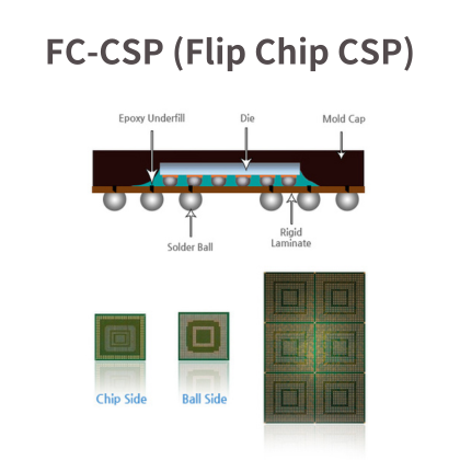
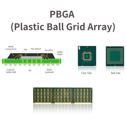
■ FCCSP
The substrate design can have both Bond Finger and Bump Pad or only Bump Pad according to the requirements. IC packaging can have both wire bonding and flip chip packaging methods. Such products can be applied to products with small package size and high electrical requirements, such as mobile devices, network equipment, smart phones, consumer electronics, digital video broadcasting, etc.
■ Flip Chip
The characteristic is that there is no Bond Finger on the front but a Bump Pad. During packaging, the chip connection point has a bump, and then the chip is flipped over so that the bump is directly connected to the substrate. It is widely used in microprocessor packaging, and has also become the first choice for packaging substrates such as high-speed graphics cards (GPUs), application-specific chips (ASICs), and computer chipsets (CPUs).
■ LGA
Generally used for radio and mobile phone frequency transmission, it is the most important element in the field of wireless communications, such as power amplifier modules, radio transceivers, Bluetooth functions and other products. In addition, the handheld device is equipped with multi-chip stacked embedded memory modules.
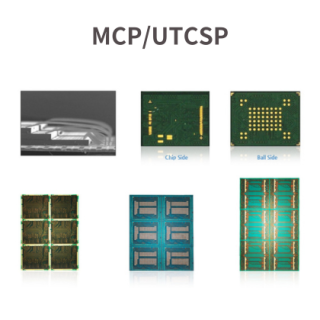
■ FBGA/MCP
Substrates used for ICs in wireless communications, mobile devices or consumer electronics products.
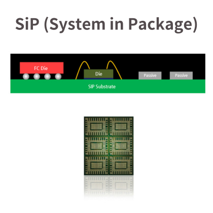
■ SiP
Provide semi-system-level packaging technologies such as heterogeneous chip packaging integration, power management modules, micro-electromechanical devices, biosensing, WiFi/Bluetooth modules, etc. to meet the needs of thin, light and compact products.
The substrate design can have both Bond Finger and Bump Pad or only Bump Pad according to the requirements. IC packaging can have both wire bonding and flip chip packaging methods. Such products can be applied to products with small package size and high electrical requirements, such as mobile devices, network equipment, smart phones, consumer electronics, digital video broadcasting, etc.
■ Flip Chip
The characteristic is that there is no Bond Finger on the front but a Bump Pad. During packaging, the chip connection point has a bump, and then the chip is flipped over so that the bump is directly connected to the substrate. It is widely used in microprocessor packaging, and has also become the first choice for packaging substrates such as high-speed graphics cards (GPUs), application-specific chips (ASICs), and computer chipsets (CPUs).
■ LGA
Generally used for radio and mobile phone frequency transmission, it is the most important element in the field of wireless communications, such as power amplifier modules, radio transceivers, Bluetooth functions and other products. In addition, the handheld device is equipped with multi-chip stacked embedded memory modules.
■ FBGA/MCP
Substrates used for ICs in wireless communications, mobile devices or consumer electronics products.
■ SiP
Provide semi-system-level packaging technologies such as heterogeneous chip packaging integration, power management modules, micro-electromechanical devices, biosensing, WiFi/Bluetooth modules, etc. to meet the needs of thin, light and compact products.
Vendor:SIMMTECH
Country:Korea
Charlie Pan
E-mail: charlie_pan@niching.com.tw
TEL: +886-7-8618808 ext.63611